Recent Progress of 40 GHz high-speed
LiNbO3 optical
modulator
Makoto Minakata
Research
Institute of Electronics, Shizuoka University / Hamamatsu,
Japan
ABSTRACT
This paper describes the recent progress and status of 40 GHz
high-speed LiNbO3 optical modulators,
and newly designed two types - a backslot type and a ridge type-
LiNbO3 optical modulators with
high-speed and low-switching voltage. The backslot is formed on the backside of
LiNbO3 substrate by using
micro-machining laser etching. The backslot type modulator is designed,
fabricated and characterized. The ridge type modulator with an overhanged upper
electrode is also calculated. The properties of the designed two types
modulators, effective refractive index for the modulation wave
nm,
modulation bandwidth fm, overlap integral Γ and switching voltage
Vπ are calculated. The optimum properties of the backslot type modulator,
fm=73GHz and the switching voltage Vπ=2.8V is calculated , and
fm=130GHz and Vπ =1.9V is achieved for the ridge type modulator at a
wavelength 1.5μm. The fabricated backslot type modulator achieved the optical
3dB bandwidth fm≧28GHz and the driving voltage Vπ
=2.8V.
Keywords: Optical modulator, ridge waveguide,
traveling-wave electrode, LiNbO3, Mach-Zehnder,
velocity-matching
1. INTRODUCTION
Advancements in the Internet, cellular-phones, and multimedia
communications have increased the needs for large-capacity optical transmission
systems. Up to now, TDM single channel 640Gbit/s transmission experiments over
60 km have been accomplished [1], and 3 Tbit/s (160 Gbit/s x 19 channel) optical
TDM and WDM transmission experiment has been reported [2]. In the near future,
Single-carrier 40 Gbit/s optical transmission systems will soon be available to
support " Information Technology". The LiNbO3 (hereafter LN) optical modulator with traveling-wave electrode and
Mach-Zehnder optical waveguide is a promising device for such high-speed
systems, because the low-frequency chirp, wide bandwidth and low-switching
voltage are practicable. In this paper, I would like to introduce the recent
progress and status of these devices. Recently, general information and status
of modulators in detail have been reported , please refer to them
[3-4].
Up to now, broad-band LN optical waveguide modulators by using a traveling-wave type electrode or
a coded phase reversal type electrode have been developed [5-9]. To realize more
efficient and extremely broad-band modulators, studies on traveling-wave devices
have been made successfully in the world. In this paper, two types novel LN
traveling-wave modulators with 3-dimensional structures - a backslot type and
a ridge type- are proposed, and basic experimental results are reported.
This modulator can satisfy the perfect velocity matching condition
between an optical wave and a modulating wave. Therefore an extremely wide-band
optical modulator can be realized theoretically, which is restricted by the
electrode loss or dispersion [8]. The ridge type modulator is also high
efficient, because it has a large overlap internal factor between the optical
wave and applied electric field [3]. To confirm the basic performance, the
backslot type modulator was fabricated and characterized. The important
microwave index was determined by the measurement of Time Domain Refractometry.
These results show that the modulating wave gains in speed and closes to the
optical wave. The modulation frequency was confirmed more than 28 GHz and the
driving voltage of 2.8V at a wavelength 1.5μm.
2. LIMITATION FACTORS OF MAXIMUM MODULATION
BANDWIDTH
For a traveling-wave optical waveguide modulator, the maximum
modulation band-width is generally limited by ・ the threshold frequency of the
electrooptical effect, ・ velocity mismatching (the propagation speed difference)
between an optical wave and a modulating wave (for example, applied electrical
field in microwave), ・ the electrode loss in the high-frequency field, and ・
structural dispersion and material dispersion [3]. Since electrooptic effect
functions in a wide frequency range from DC to infrared (THz), factor ・ is no
problem. Factor ・ to ・ depend on the electrode and its structure. Among them,
the achievable bandwidth is mainly restricted by velocity mismatching. A
modulation bandwidth fm of the modulator is reversely proportional to the
difference between an optical wave velocity Vo= c/no and a modulating wave
velocity Vm= c/nm, where c is a velocity of light, and no, nm is
refractive index for an optical wave and a modulating wave, respectively. The
bandwidth also increases as an electrode length l is decreased at the expense of
a large drive power. Thus, 3dB-down modulation band-width
fm is
proportional to 1/(Vo-Vm) l, as shown in Fig.1. For a modulator with a
coplanar traveling-wave electrode (see Fig.1), Vo is 1.95 times faster than Vm (no=2.15,
nm=4.2). Therefore, the product of
fml is
limited to 9.2GHzcm[5].
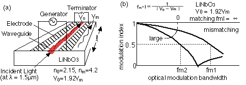
Figure 1: A modulator with a co-planar traveling-wave electrode(a),
and the definition of the modulation bandwidth fm (b).
For example, in the directional coupler type device with
l=2.5mm, fm=40GHz and a switching voltage Vπ=26V( at a wavelength
λo=1.5μm) was reported as shown in Fig.2 [10]. If the perfect velocity
matching condition of Vo=Vm is
satisfied, the bandwidth fm is theoretically infinite. However, the
bandwidth is limited by the electrode loss even under the perfect velocity
matching condition. For example , when copper electrodes are used at 100 GHz,
the microwave skin depth δ is 0.2μm because of the high conductivity of
copper[11]. In this case, slight roughness in the electrode surface causes
scattering and radiation loss. Therefore, mirror finish of electrode is
required. Although the electrode is mirror-finished, the dimensions of the
electrode cross section are finite and the microwave attenuates in proportion to
exp(−αl). Therefore, the attenuation increases with an increase of l.
The
material dispersion of LN mentioned in factor ・ is almost constant at
frequencies up to 300GHz. In the electrode construction where the TEM wave
approximation holds, it is believed to be constant at frequencies up to at least
200GHz.
On the other hand, the upper limit of optical modulation frequency
and the modulation voltage are inversely proportional to the electrode length.
Therefore, it is difficult to fabricate a high-speed and wideband optical
modulator using low driving voltage.
To overcome this problem -velocity
mismatching limitation and trade off-, many efforts have been made [5-9] as
shown in Fig.1. For a modulator with a coplanar traveling-wave electrode (see
Fig.1), Vo is 1.95 times faster than Vm (no=2.15, nm=4.2). Therefore, the product of fml is limited to
9.2GHzcm[5].

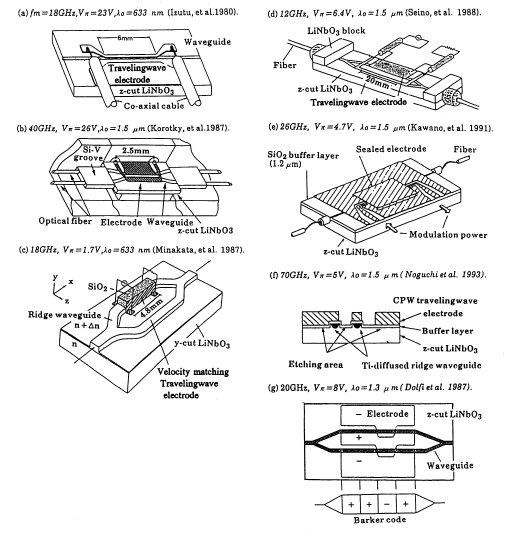
Figure 2:
Recently developed wideband optical modulators.
Fig.2. In methods (a) to (f) [7,10,11,12,6,13], the modulation
wave velocity should be close to the velocity of light to achieve wide
bandwidth. In case (g), the electrode structure is coded to diffuse the
spectrum, resulting in the achievement of wideband[9]. In case (e), a ridge
waveguide is used, where the 3 dB-down bandwidth is 70GHz and Vπ=5V [13]. An
optical modulator with YBaCuO-based superconducting electrodes was reported. The
electrode loss at 77K is 10-3 of those of Cu and Al. In this device,
the center frequency is 18GHz and Vpp=2.3V[14]. Optical modulation at 94 GHz was
achieved by coupling a dielectric tapered guide and electrode
antenna[15].
3. A PROPOSED TRAVELING-WAVE OPTICAL MODULATOR
-Backslot Type-
3.1 Velocity matching
The proposed
modulator -backslot type-, shown in Fig.3, is composed of a planar waveguide, a
traveling-wave electrode and a backside slot. By changing the thickness of the
substrate, the microwave index nm is
considerably decreased, and the applied electric fields is increased. The
reasons are as follows; 1) the electric field leaks out effectively into the
backside (air) so that nm decreases to
be satisfied the perfect velocity matching conditions, 2) an overlap integral
Γ is about 2 times larger than that of the existing planar electrode
modulator with a thick buffer layer (see Fig.3(b)). The Configuration of actual
designed device is shown in Fig.4 with a CPW electrode.
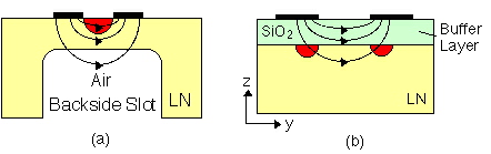
Figure 3: (a) The proposed LiNbO3
modulator structure with a backside slot, and (b) the conventional planar type
modulator structure with SiO2 buffer layer.

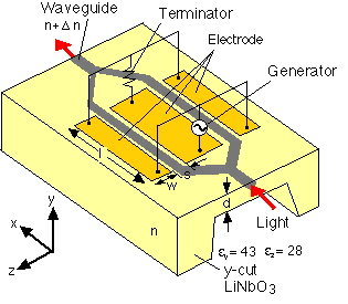
Figure 4:
Schematic diagram of the proposed modulator. The element is the Mach-Zehnder
intensity optical modulator with the CPW traveling-wave electrode. Backside of
the substrate is etched to achieve the velocity matching.
3.2 Electrode loss and dispersion
In the range from
microwave to millimeter wave, the electrode loss increase with an increase in
frequency cased by the skin-effect [3]. The electrooptically induced "optical
phase shift" which is integrated along the electrode length is reduced with an
increase in electrode loss. Thus, the bandwidth is reduced by the electrode
loss. Under the perfect velocity matching condition [3], achievable modulation
bandwidth fm is given by
fmloss=(6.84/α0l)2 (1)
where α0 is an attenuation
constant of the modulation microwave. Furthermore in the designed modulator, the
actual bandwidth is less than a limited bandwidth based on the structural
dispersion and the material dispersion [3].
4. DESIGN OF THE MODULATOR (1) - Backslot
Type -
4.1 nm and fm
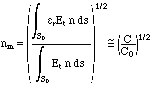
A
wavelength of microwave is fair longer than the electrode gap. For example, when
the electrode gap is 10 μm and the wavelength is about 2mm at frequency 100 GHz.
Therefore we assume that modulating wave is a transverse electric and magnetic
wave. That is Ex=Hx=0. By this assumption, nm is given by eq.(2),

(2)
where εr is relative dielectric constant and
S0 is
the cross section including the one-side electrode per unit length. n is
a unit vector perpendicular to ds. Et is the transverse electric
field induced by applied modulation voltage. C is a capacitance per unit
length of the modulator, and C0 is a capacitance when only the electrode is existing
in air. Here, Et is

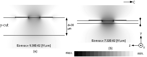
Figure 5: The applied electric field of z-component distribution
calculated by the SOR method for (a) substrate thickness d=30 μm, (b) d=5μm for
y-cut (or x-cut) LiNbO3 substrate, respectively
given by
the potential distributionΦ. Φ is calculated by
Laplace's equation:
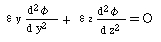 (3)
(3)
and solved by a successive over relaxation (SOR) method
[3]. ・Et・and its distribution are calculated based on Φ as shown
in Fig.5. When the propagation microwave is lossless [3], fm is given by
 (4).
(4).
4.2 Vπ and
Γ
Switching voltage (halfwave voltage) Vπ is given by

(5)
where wavelength λ is the
wavelength of light, S is the electrode gap, r33 is the electrooptic coefficient.
Γ is the overlap integral factor between the applied electric
field E (y, z) and the optical electric field ε(y,z), and given by

(6)
where E is
an applied average electric field. ε(y,z) is calculated by combining an
effective index method[3]. The using relative index difference is
6.5x10⁻³ and the depth of waveguide is 2μm. E(y,z) is the
transverse electric field calculated by the SOR method (shown in
Fig.5).
4.3 Calculated Results
Figure 6 shows the relationship
between the bandwidth and the substrate thickness normalized by electrode gap S.
Where αo is an attenuation constant of the modulation microwave, and depends on
the electrode conductivity and geometry.
When the d/S=0.19 for y-cut, and
0.12 for z-cut, no=nm=2.15. That is, the perfect velocity matching
conditions is satisfied, the maximum value of fm is obtained 292 GHz
with l=10mm, on both cut of the substrate. Figure 7 shows the relationship
between Vπ and the substrate thickness d. The concentration of the z
component electric field is strongly depend on the substrate direction. The
y-cut substrate has much better concentration as compared with the z-cut, with a
decrease in d. Table 1 shows the calculated relationship between a
substrate thickness and characteristics. Where we assume the Mach-Zehnder type
switch as shown in Fig.4, and Au electrode is used at a 1.5 μm wavelength. The
designed modulator for y-cut (x-cut) substrate has a broad bandwidth and high
efficiency compared with existing modulators. The optimum properties fm
=73 GHz and Vπ=2.8V at a wavelength 1.5μm, is achieved for the y-cut (x-cut)
LiNbO3 substrate, with l=20 mm, d=3.8μm, under the perfect velocity matching
condition.
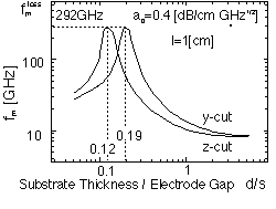
Figure 6: The
relationship between modulation bandwidth fm and d/S (substrate thickness
/ electrode gap) for y-cut and z-cut LiNbO3 substrate, for αo= 0.4 dB/cm
GHz1/2 and l = 1 cm.
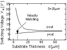
Figure 7: The
relationship between switching voltage Vπ and substrate thickness d for y-cut
and z-cut LiNbO3.
Table 1: The
values of the modulation bandwidth fm, switching voltage Vp and substrate
thickness d for y-cut and zcut LiNbO3 substrate (S=20nm, l=2cm,αo=0.4dB/cm
GHz1/2).

4.4
Experimental
To confirm the basic performance, a x-cut LN substrate
backside-etched modulator was fabricated and characterized. The optical
waveguide was fabricated using x-cut LN substrate by the Ti diffusion method.
The CPW electrode was directly electroplated to the substrate. The gap S=40μm,
the width of the center electrode w=30μm, and the interaction length l=40 mm,
respectively. The backside slot was fabricated by KrF excimer laser ablation.
The cross-section of the modulator is shown in Fig.8. Less than 10μm thickness
of LN substrate just under the traveling wave electrode have been fabricated.
The end faces of the modulator were polished and pigtail fibers were
successfully connected by using ultraviolet-cured adhesive. From measured TDR
(Time Domain Refractometry) characteristics date, it is clear that the microwave
in the modulator with backside slot has less shorter traveling-time compare to
the modulator which has the same dimension and no backside slot. That is, the
microwave propagation speed Vm along the optical waveguide is higher than that
without backside slot. The modulator with backside slot has also high impedance
compare to that one.
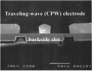
Figure 8: The cross-section SEM photograph of the fabricated
modulator with a backside slot.
Then, to confirm
the modulator performance, the S-parameters, S11 and S21, of the modulator are
measured up to 25GHz by a vector network analyzer. S11 is below -10 dB over the
entire frequency range, since the impedance matching is sufficient. S21 is shown
to be smooth and the conductor loss is very low. Fig.9 shows the frequency
response of the fabricated modulator. Based on these results, the parameters
nm, Zo, and αo are calculated to be
2.25, 45.6 ohm, and 0.2 dB/cmGHz1/2, respectively. The optical 3 dB
bandwidth is higher than 28GHz by calculated from S-parameter, and the half-wave
voltage Vπ is 2.8V at a wavelength l =1.5μm. Measured extinction ratio is 25 dB,
and the total insertion loss is 6.1dB.
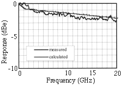
Figure 9: Frequency response of the fabricated
modulator.
5. DESIGN OF THE MODULATOR (2) - Ridge Type -
This section describes another proposed design of the ridge type optical
modulator with an overhanged upper electrode to achieve the high-speed and
low-switching voltage as shown in Figure10. The conventional ridge structure is
effective to lower the switching voltage[3,13].The proposed structure makes use
of the ridge type for low-switching voltage, and is simultaneously aiming at
the perfect velocity matching and low-electrode loss to achieve the
high-speed modulation.
We calculated the distribution of the applied
electric field by using the successive over relaxation(SOR) method (see Figure
11).The properties of the designed modulator, effective refractive index for the
modulation wave nm , modulation
bandwidth fm , overlap integralΓ,
switching voltage Vπ and the
characteristic impedance Z0 ,
are calculated based on the electric field and the optical intensity
distribution as shown in Figure 12-15.The optimum design parameters to give the
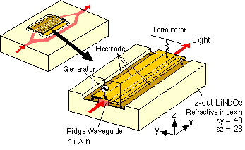
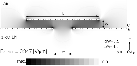
Figure 10: The
proposed modulator structures on the z-cut LiNbO3 substrate with the overhanged upper electrode. The structure is formed
on only one of the waveguide of the Mach-Zehnder intensity optical modulator
with the traveling-wave type electrode.

Figure 11: The z-direction component of
the applied electric field calculated by the succesive-over relaxation method
for the ridge type modulator ,where dr/w=0.5 and L/w=4.0
.

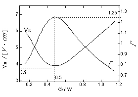
Figure 12: The plot of
Vpl (product of switching voltage and electrode length) and
overlap integral Γ versus dr/w for the ridge type .
Figure
13: The relationship between effective refractive index for the modulation wave
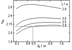
nm, L/w and dr/w for the ridge type (1). The velocity
matching (nm=no) is achieved for L/w=3.9 and
dr/w=0.5 , shown as the dotted line.
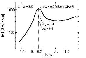
Figure 14: The relationship between
modulation bandwidth fm and dr/w (L/w=3.9) for the ridge
type . The velocity mismatching and the electrode loss terms are included in the
calculation.
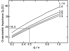
Figure 15: The relationship between
characteristic impedance Z0, L/w and dr/w for the ridge
type (1). Z0 becomes 18.4Ω for the optimum design (L/w=3.9 and
dr/w=0.5) .
Table 2: The values of the bandwidth,
switching-voltage and performance index for planar-type, back slot-type,
ridge-type structure (l =2cm).
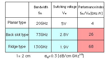
highest-speed modulation and the lowest-switching voltage
are dr/w=0.5 and L/w=3.9 for
the ridge type, where dr :
the ridge height,w : the ridge width and L : the upper electrode width. For the
electrode length (l =2cm) and the electrode loss constant (a0=0.3dB/cmGHz1/2),obtained
properties of the designed modulator are fm=130GHz,Vπ=1.9V and
performance index fm/ Vπ= 68 GHz/V.These properties are superior to the conventional LN
modulators with the planar type electrodes, where the typical value of
fm/Vπ is 4 GHz/V. In
summary, Table 2 shows the calculated properties of the backside slot type and
the ridge type modulator.
6. CONCLUSION
The recent progress and status of 40 GHz high-speed LiNbO3 optical modulators have been described . Limitation
factors of the high-speed / broad-band LN modulators have been discussed. The
efficient and broad-band LiNbO3 optical modulator with
3-dimensional novel structures have been proposed. These constructions can be
obtained perfect velocity matching between the optical wave and the modulating
wave. Therefore an extremely wide-band optical modulator can be realized
theoretically. The calculated values of the well designed backside slot type
modulator was fm=73 GHz and Vπ=2.8V for the y-cut (x-cut)
LiNbO3 substrate, and the well designed
ridge type modulator was fm=130GHz,
Vπ=1.9V at a wavelength
1.5μm,with l=20 mm.
ACKNOWLEDGMENTS
The author would like to thank Dr.A.K.Dutta and Prof. Y. Hatanaka for
valuable recommendation, and to Dr. M.Goto and H.Awano for many calculations and
valuable support, and also to Dr. M. Imaeda, J.Kondo, A.Kondo, K.Aoli, O. Mitomi
and Y.Kozuka for calculation and fabrication of the backslot modulator. Part of
this work is supported by Monbukagakusho Grant-in-Aid for Scientific Research
(11450139).
REFERENCES
1. M.Nakazawa et. al., " TDM single channel 640Gbit/s transmission
experiments over 60 km using a 400 fs pulse train and a walk-off free,
dispersion-flattened nonlinear optical loop mirror," Tech.Digest of
OFC'98,PD-14, 1998.
2. S.Kawanishi et.al.," 3 Tbit/s optical TDM and WDM transmission
experiment ,"Electron Lett.,35,pp.826-827, 1999.
3. M.Minakata,"LiNbO3 optical wavegude devices," Electronics and
Communications in Japan, Part2,77, pp.37-51, 1994. Translated from
Denshi Joho Tsusin Gakkai
Ronbunshi,77-C-1,pp.194-205,1994.
4. N.Dagli," Wide-bandwidth laser and modulators for RF
photonics,"IEEE Trans.Microwave Theory and Technol.,MTT-47,
pp.1151-1171,1999.
5. R.C.Alferness, "Waveguide electrooptic modulators,"IEEE
Trans.Microwave Theory and Tech.,MTT-30, pp.1121-1137, 1982.
6. K.Kawano,K.Kitoh,H.Jumonji,T.Nozawa and M.Yanagibashi,"New
traveling-wave electrode Mach-Zehender optical modulator with 20 GHz and 4.7V
driving voltage at 1.52μm wavelength,"
Electron.Lett.,25,pp.1382-1383,1989.
7. T.Sueta and M.Izutsu,"1.11 High speed guided-wave optical
modulators," Optical devices and Fibers (Ed.by Y.Suematsu),pp.140-150,Ohm
& North-Holland Pub.,1982.
8. M.Minakata,"LiNbO3 broad-band optical modulator (Invited)," Third
Optoelectronics Conf. (OEC'90) Tech. Digest, pp.136-137,1990.
9. M.Nazarathy,D.W.Dolfi,andR.J.Jungerman,"Spread spectrum frequency
response of coded phase reversal travering wave modulators,"J.Lightwave
Technol.,LT-5,pp.1433-1443,1987.
10. S.K.Korotky et.al.," Optical intensity modulation to 40GHz using a
waveguide electrooptic switch,"Appl.Phys.
Lett.,50,pp.1631-1633,1987.
11. K.Miura,M.Minakata and K.Kawakami,"Ridge modulator
1987,"CLEO'87
12. M.Seino et.al.,"12GHz bandwidth Ti:LiNbO3 Mach-Zehnder modulator,"
Second Optoelectronis Conf.(OEC'88), Post-deadline Papers,PD-1,1988.
13. K.Noguchi, O.Mitomi,H.Miyazawa and S.Seki,"A broadband Ti:LiNbO3
optical modulator with a ridge structure," J. Lightwave
Technol.,13,pp.1164-1168,1995.
14. K.Yoshida et.al.,"A study on LN light modulatorusing the YBa2Cu3Oy
superconducting electrode," IEEE Trans.
Electron.,E-75-C,pp.65-69,1992.
15. F.T.Sheeky,W.B.Bridges, and H.Schaffner,"60GHz and 90GHz
antenna-coupled LNelectrooptic modulators," IEEE
Photon.Technol.Lett.,5,pp.307-310,1993.
業績リストに戻る