Effect of Control-Ring on
LiTaO3 Domain Inversion
by Electron Beam
Irradiation
Makoto Minakata, Haruyuki
Awano and Yoshikazu Nakada
Research Institute of Electronics, Shizuoka
University
3-5-1 Johoku, Hamamatsu 432-8011, JAPAN
Phone & Fax :
+81-53-478-1336
E-mail : h-awano@rie.shizuoka.ac.jp
Abstract - The control-ring was drawn on LiTaO3
crystal utilizing various electronic density before a small-dot drawn. The size
of inversion domains was zero under the condition of no ring, 13μm under the
condition of middle density, and 29μm under the high density. Thus, we can
confirm "the interaction of Coulomb" induced by the injected
electrons.
I. INTRODUCTION
We have been studying the formation of nanometer scale inversion domains in
LiTaO3 using electron beam (EB) irradiation(1). Therefore, a control of nanometer scale domain
inversion realizes new opto-electronic devices such as an ultrahigh density
memory(2) (〜1 Tb/cm2).
In this paper, we report for the first time
"the interaction of Coulomb" caused by the electrons impinging into a crystal by
EB irradiation. Actually we showed the existence of "the interaction of Coulomb"
between a small-dot and a surrounding ring (control-ring) which is drawn with
various electronic density before a small-dot drawn.
II. EXPERIMENT
II-1. Electron beam irradiation mode and domain structure
 The experimental setup for EB scanning is composed
of a scanning electron microscope (SEM), a pattern generator and a computer. The
beam spot is 10 nm in diameter, and the irradiated position is controlled by 10
nm(1). We used a LiTaO3
crystal of 500μm thickness and the +Z surface was coated with Au film. The free
-Z surface is irradiated with a scanned EB. The EB acceleration voltage, current
and clock were 20 kV, 200 pA and 1〜30,000, respectively. Clock means electron
irradiation time. "Clock 1" is correspond to 0.5μs. Therefore "clock 30,000" is
equivalent to 15 ms. After chemical etching, the pit on +Z surface is observed
because etching rate of the -Z face is much higher than that of the +Z face.
Consequently, the pit size is corresponding to the inversion domain area(3).
The experimental setup for EB scanning is composed
of a scanning electron microscope (SEM), a pattern generator and a computer. The
beam spot is 10 nm in diameter, and the irradiated position is controlled by 10
nm(1). We used a LiTaO3
crystal of 500μm thickness and the +Z surface was coated with Au film. The free
-Z surface is irradiated with a scanned EB. The EB acceleration voltage, current
and clock were 20 kV, 200 pA and 1〜30,000, respectively. Clock means electron
irradiation time. "Clock 1" is correspond to 0.5μs. Therefore "clock 30,000" is
equivalent to 15 ms. After chemical etching, the pit on +Z surface is observed
because etching rate of the -Z face is much higher than that of the +Z face.
Consequently, the pit size is corresponding to the inversion domain area(3).
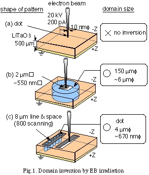
There was no etching pattern when a point was
drawn at clock 30,000 (Fig.1(a)). When the small rectangle patterns were drawn
at clock 30,000, domain inversions were not occurred less than 540 nm square
patterns. In the case of 2μm to 550 nm square, it was obtained the circular
inverted patterns which size were 150〜6μm in diameter (Fig.1(b)). When the 8μm
line & space pattern was drawn in 500μm square, the domain inversion
occurred in segmented regions(3) (Fig.1(c)).
 II-2. Domain structure
using control-ring
II-2. Domain structure
using control-ring
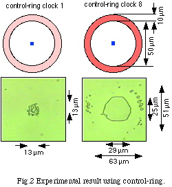
The control-ring was drawn with the size of 50μm
in inside diameter and 10μm in width utilizing various electronic density.
Subsequently the small rectangle pattern was drawn. After etching, the pit size
on +Z surface was zero under the condition of no ring, 13μm under the condition
of middle density (clock 1), and 29μm under the high density (clock 8), as shown
in Fig.2. Thus, we can confirm "the interaction of Coulomb" induced by the
injected electrons. At this point, we considered the strength for the
interaction of Coulomb(4).
III. DISCUSSION
 It has been discovered that the
relation between the quantity of the charges by EB irradiation V and the size of
etch pit (inverted region) D is able to be expressed by using the cone
model(3). It is considered that the charge
distribution of irradiated/injected electrons is formed the shape of cone which
has a fixed vertical angle a. By using this model, there are two threshold at
domain inversion, one is the nuclear formation threshold hn
(= 204 kV/cm) and the other is the inversion area enlarged threshold hth (= 120 kV/cm)(3). In domain
inversion using EB irradiation, when an electric field value induced by injected
electrons is higher than the value of hn, a domain inversion
occurs and the area of inverted domain is enlarged until the induced field is
less than the value of hth.
It has been discovered that the
relation between the quantity of the charges by EB irradiation V and the size of
etch pit (inverted region) D is able to be expressed by using the cone
model(3). It is considered that the charge
distribution of irradiated/injected electrons is formed the shape of cone which
has a fixed vertical angle a. By using this model, there are two threshold at
domain inversion, one is the nuclear formation threshold hn
(= 204 kV/cm) and the other is the inversion area enlarged threshold hth (= 120 kV/cm)(3). In domain
inversion using EB irradiation, when an electric field value induced by injected
electrons is higher than the value of hn, a domain inversion
occurs and the area of inverted domain is enlarged until the induced field is
less than the value of hth.
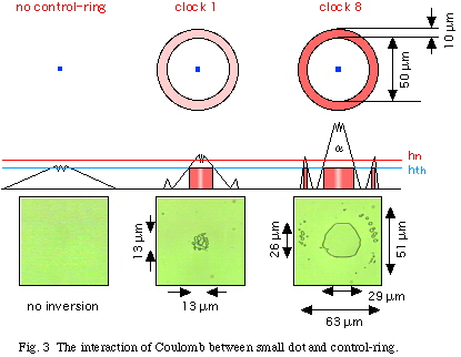
 Fig.3 shows the interaction of Coulomb between
small dot and control-ring by using two threshold. Under the condition of "no
control-ring", insufficient charge density did not induce the domain inversion.
As the surface resistivity on the crystal reduces on the electron irradiated
area, irradiated electrons may be able to move. The charges irradiated into the
center of the control-ring is gathered toward the center by the interaction of
Coulomb. As an electric field value induced by injected electrons is higher than
the value of hn, a domain inversion occurs and the area of
inverted domain is enlarged until the induced field is less than the value of
hth. More excessive charges extend the inversion area of
center dot by means of more stronger interaction. In the area on the
control-ring, domain inversion may partially occur, because an electric field
value is higher than the value of hn.
Fig.3 shows the interaction of Coulomb between
small dot and control-ring by using two threshold. Under the condition of "no
control-ring", insufficient charge density did not induce the domain inversion.
As the surface resistivity on the crystal reduces on the electron irradiated
area, irradiated electrons may be able to move. The charges irradiated into the
center of the control-ring is gathered toward the center by the interaction of
Coulomb. As an electric field value induced by injected electrons is higher than
the value of hn, a domain inversion occurs and the area of
inverted domain is enlarged until the induced field is less than the value of
hth. More excessive charges extend the inversion area of
center dot by means of more stronger interaction. In the area on the
control-ring, domain inversion may partially occur, because an electric field
value is higher than the value of hn.
In
the cone model, it has been considered that the cone has a fixed vertical angle.
However, this angle may be changed in consequence of using control-ring.
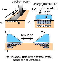
In
Fig.1(c), to draw the line pattern by EB, it needs to consider the interaction
of Coulomb as shown in Fig.4. It has been explained that charges on 2 lines
repel each other(3). This explanation is
supported by the experiment of line pattern drawing.
IV. CONCLUSION
In the domain inversion by EB irradiation, we report for the first time "the
interaction of Coulomb" caused by the electrons impinging into a crystal.
Actually we showed the existence of "the interaction of Coulomb" between a
small-dot and a control-ring.
REFERENCES
(1) M. Minakata, Y. Nakada and H. Awano, Extended Abstracts (The 44th Spring
Meeting,1997); The Japan Society of Applied Physics and Related Societies.
30p-NF-12.
(2) M. Minakata, Y. Nakada and T. Nomura, Proceedings of
JICAST'98/CPST'98, 245-248(1998).
(3) M. Minakata, Y. Nakada and H.
Awano, Bulletin of the Research Institute of Electronics Shizuoka University,
32,49-57
(4) M. Minakata, Y. Nakada and H. Awano, Extended Abstracts (The
60th Autumn Meeting,1999); The Japan Society of Applied Physics.
2p-ZB-5.
業績リストに戻る
 The experimental setup for EB scanning is composed
of a scanning electron microscope (SEM), a pattern generator and a computer. The
beam spot is 10 nm in diameter, and the irradiated position is controlled by 10
nm(1). We used a LiTaO3
crystal of 500μm thickness and the +Z surface was coated with Au film. The free
-Z surface is irradiated with a scanned EB. The EB acceleration voltage, current
and clock were 20 kV, 200 pA and 1〜30,000, respectively. Clock means electron
irradiation time. "Clock 1" is correspond to 0.5μs. Therefore "clock 30,000" is
equivalent to 15 ms. After chemical etching, the pit on +Z surface is observed
because etching rate of the -Z face is much higher than that of the +Z face.
Consequently, the pit size is corresponding to the inversion domain area(3).
The experimental setup for EB scanning is composed
of a scanning electron microscope (SEM), a pattern generator and a computer. The
beam spot is 10 nm in diameter, and the irradiated position is controlled by 10
nm(1). We used a LiTaO3
crystal of 500μm thickness and the +Z surface was coated with Au film. The free
-Z surface is irradiated with a scanned EB. The EB acceleration voltage, current
and clock were 20 kV, 200 pA and 1〜30,000, respectively. Clock means electron
irradiation time. "Clock 1" is correspond to 0.5μs. Therefore "clock 30,000" is
equivalent to 15 ms. After chemical etching, the pit on +Z surface is observed
because etching rate of the -Z face is much higher than that of the +Z face.
Consequently, the pit size is corresponding to the inversion domain area(3).